
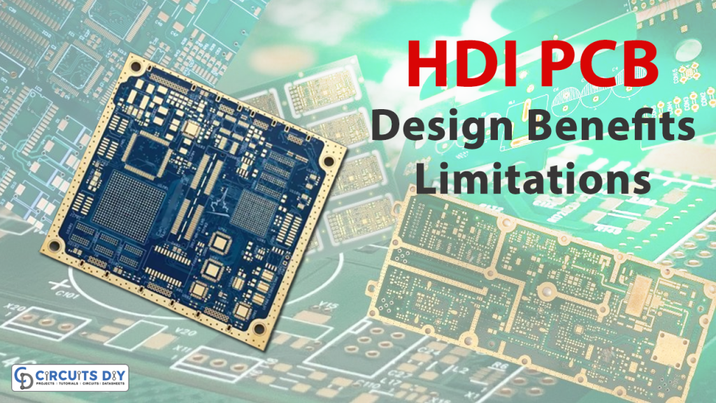
High-Density Interconnect (HDI) PCBs represent a significant advancement in produced world table technology, giving superior efficiency in lightweight electronic devices. Unlike conventional PCBs, HDI PCBs leverage sophisticated manufacturing techniques to accomplish higher enterprise densities and smaller form factors. This allows for the integration of more components and functionality in to a smaller space, creating them suitable for purposes wherever size and weight are important factors.
One of many essential top features of HDI PCBs is their utilization of microvias, which are microscopic holes drilled in to the PCB substrate to create associations between different layers of the board. These microvias enable better redirecting of signs and energy, lowering indicate reduction and improving overall electrical performance. Additionally, HDI PCBs can integrate multiple levels of circuitry, more improving their operation and flexibility.
The compact measurement and high-density design of HDI PCBs also donate to increased indicate reliability and reliability. With smaller indicate routes and paid off electromagnetic interference, HDI PCBs may support higher-speed knowledge sign and more complex digital designs. That makes them well-suited for use within advanced electronics such as for example smartphones, pills, wearables, and automotive systems.
In addition to their electrical efficiency benefits, HDI PCBs present benefits when it comes to manufacturing effectiveness and cost-effectiveness. By consolidating multiple components onto just one board, HDI PCBs lower the need for extra assembly steps and interconnects, streamlining the manufacturing process and decreasing over all production costs. Additionally, their smaller measurement and lighter fat may result in savings on substance and delivery expenses.
HDI PCB technology continues to evolve fast, driven by the demand for smaller, more powerful digital devices. Innovations such as stacked microvias, successive lamination, and laser drilling are driving the boundaries of what is probable with HDI PCBs, allowing even greater degrees of integration and performance. As a result, HDI PCBs are positioned to play a main role in the progress of next-generation electronics across a wide selection of industries.
Despite their several benefits, planning and manufacturing HDI PCBs may provide difficulties, especially in terms of design, impedance control, and thermal management. Manufacturers must cautiously contemplate facets such as for instance signal reliability, high frequency pcb distribution, and portion positioning to ensure optimal efficiency and reliability. Moreover, the use of advanced manufacturing methods such as laser drilling and constant lamination involves specialized gear and expertise.
Over all, HDI PCBs represent an important development in produced enterprise table technology, providing a variety of high performance, lightweight size, and cost-effectiveness which makes them well suited for a wide selection of applications. As electronics continue steadily to become smaller, lighter, and stronger, the need for HDI PCBs is expected to develop, driving more innovation in the field.